The optical Vortex phase plate is a unique optic, whose structure is composed entirely of helical or spiral phase steps, whose purpose it is to control the phase of the transmitted beam. The winding “staircase” surface structure is depicted in the Figure 1 immediately below:

Figure 1: Winding “Staircase” surface profile of diffractive vortex phase plate.
The total etching depth from the top to bottom of “staircase” is a function of the design wavelength and the substrate’s optical index. Generally, this depth is of the same order of magnitude as the design wavelength.
Therefore, each optical Vortex phase plate is wavelength specific.
If a customer wishes to use an optical vortex phase plate for a slightly shifted wavelength, we can simulate upon request what performance is expected.
The topological charge, denoted in the relevant literature as m, refers to the number of 2π cycles (i.e. “staircases”) that are etched around 360 degree turn of diffractive surface. In Fig.1 above, one “staircase” cycle covers entire 360° turn of surface, so m=1 for that vortex phase plate. In Fig.2 below, the surface profiles are illustrated for optical Vortex phase plate with m=2, m=3 and m=4.
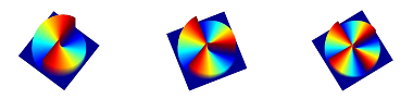
Figure 2: Surface profiles for vortex phase plates with m=2, m=3 and m=4.
One main effect of a higher topological charge is an increase in the angular moment of the vortex beam by a factor of m. Another effect is to magnify the ring intensity pattern dimensions by a factor of m, as illustrated in the below simulation.
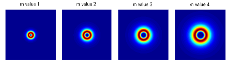
Figure 3: Simulated “far-field” intensity images of Vortex beams with variable m value.
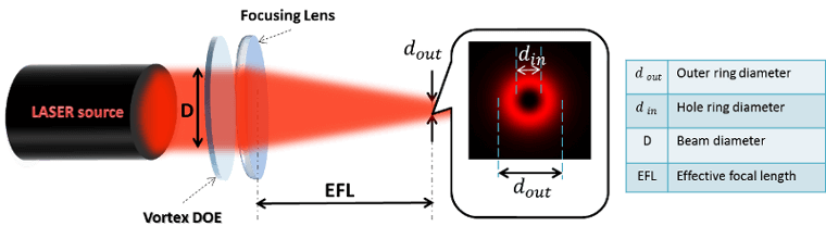
Figure 4: Typical Set-up for Vortex phase plate system.
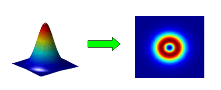
The optical Vortex requires as input a collimated Single Mode (TEM00) Gaussian input beam, which it converts to a TEM01 axially symmetric mode.
The advantage of working with a larger input beam is twofold. First, a larger beam reduces somewhat the sensitivity of the output to DOE alignment tolerances. Secondly, a larger input beam will enable achieving a smaller vortex spot, which is often a desired outcome in many applications.
The two translation stages in fig.4 above are meant to give the user precise control of elements’ locations, to reduce tolerance effects. This is discussed further in the section on Tolerances.
All optics in the beam path should be of high quality, i.e. low irregularity figure, so as not to introduce wave-front errors which could degrade performance. This includes mirrors which should have high flatness specification. Here, too, a larger beam size incident on the mirror will reduce its sensitivity to localized aberrations.
It is recommended to work with the optical vortex phase plate in the waist of the laser. Nonetheless, if the beam has a small divergence angle(<1º), there should not be any noticeable effect on the output quality, but only on the exact working distance.
If, due to mechanical or other constraints, the DOE will be located at a distance from the beam waist, it is important to take this distance into consideration, along with the beam divergence, in the designing of the DOE. Otherwise, the resultant wave-front aberration can generate an interference/ripple pattern over the output beam, whose intensity will grow as a function of the DOE’s distance from waist and the divergence angle.
When designing the desired output Vortex beam size, it is important to be familiar with the physical limits of the minimum spot size. The formula for the diffraction-limited spot diameter at 1/e2 follows:
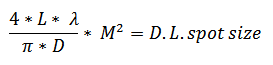
L: Working Distance
λ: Wavelength
D: Input Beam Size
M2: M2 value of input laser beam
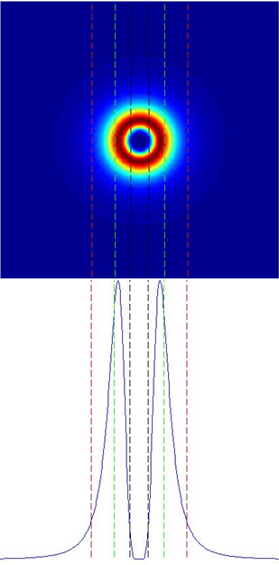
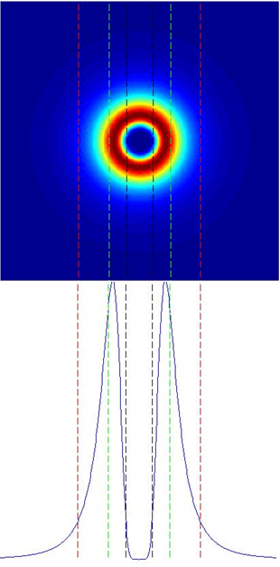
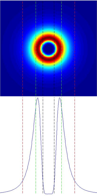
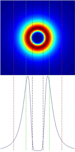
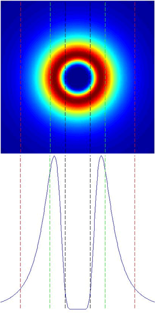
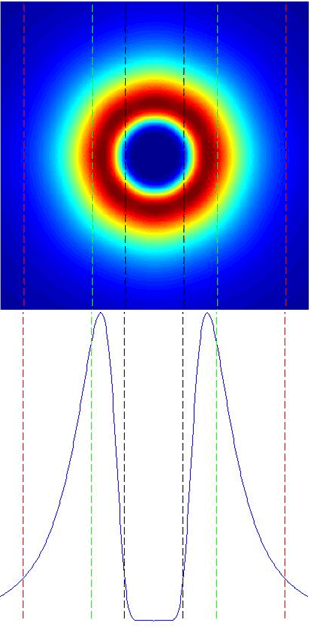
In this illustration below,the Vortex spot size at 1/e2, the size of the hole in center at 1/e2 and the transfer region will be express in term of diffraction-limits (DL) given by the above formula.
In the pictures, the vortex spot size is the distance between the two red lines, the hole size is the distance between the two black lines and the transfer region is the distance between the first red line and the first green line.
Use Holo/Or’s Vortex phase plate optical calculator to calculate output parameters for your system.
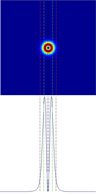
ring size: 2.0175 DL
hole size: 0.1834 DL
transfer region: 0.472 DL
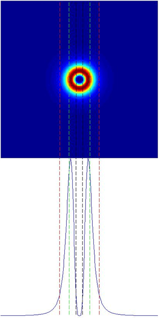
ring size: 3.013 DL
hole size: 0.4978 DL
transfer region: 0.707 DL
ring size: 4.114 DL
hole size: 0.812 DL
transfer region: 0.996 DL
ring size: 5.266 DL
hole size: 1.127 DL
transfer region: 1.31 DL
ring size: 6.472 DL
hole size: 1.415 DL
transfer region: 1.651 DL
ring size: 7.73 DL
hole size: 1.7 DL
transfer region: 1.99 DL
ring size: 8.93 DL
hole size: 1.965 DL
transfer region: 2.306 DL
ring size: 10.19 DL
hole size: 2.28 DL
transfer region: 2.65 DL
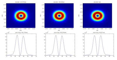
The best performance will be obtained for a well-positioned perfectly aligned part, located precisely in the plane of the nominal working distance. To illustrate the sensitivity of vortex performance to different tolerance parameters, several graphs are included here for a standard vortex phase plate (WD: 100mm, λ: 633nm).
Fig. 5: Effect of x/y axis de-centering (92um, 46um, 0um) of 8mm input beam on optical vortex phase plate
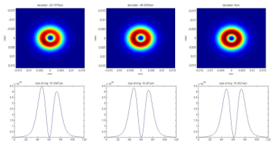
Fig. 6: Effect of x/y axis de-centering (92um, 46um, 0um) of 15mm input beam on optical vortex phase plate