Introduction: Wafer laser grooving with UV beam splitters
Semiconductor packaging is a growing application field for UV lasers in general, and especially for ultra short pulsed (USP) UV lasers. A UV grooving process is often used as a preliminary step to saw dicing in the semiconductor industry, to prevent sensitive structured from being damaged by shear forces during dicing.In this article we review how diffractive UV beam splitters, also known as multispot DOEs, enable high throughput wafer grooving in the semiconductor packaging industry.
Background: The need for laser grooving
The continuing increase in the active layer stack is driving a decrease in the Si substrate thickness, requiring increased die strength after singulation to maintain acceptable yield. Another requirement is a low side burr of less than 1-2um, as processes such as micro bump interconnect are replacing tradition wire bonding. These demands by the semiconductor packaging industry require precise laser process control, including polarization, correct wavelength choice and of course a properly tailored intensity pattern. This is where UV beam splitter optics come in.

What are UV laser beam splitters
Diffractive UV laser beam splitters are transmissive phase elements etched in fused silica that create an array of beams with predesigned angles of separation. These DOEs are different from UV plate beam splitters or cube beamsplitters, that can only split the light into two orders (transmitted and reflected at 90 deg) by using a tailored coating. Instead, these diffractive optic elements are a Damman grating type components with many orders that can generate one dimensional line arrays of spots, two dimensions square or hexagonal arrays, and even more complex patterns such as V type arrays consisting of two lines of spots with gradually decreasing separation.
Advantages of diffractive UV beam splitters compared to other optical beamsplitters
- Splitting to any number of beams
- Polarization insensitive
- Weak sensitivity to input beam tilt, up to ~10 deg
- Almost no angular tolerances
UV beam splitters contribution to semiconductor packaging
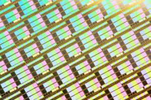
The laser grooving process often employs a preliminary stage, where two trenches are dug at the edges of the groove, before the maximum laser beam power is used to dig the main groove. This is done to prevent heat from damaging dense structures close to the dicing groove.By using a special diffractive UV beam splitter , the illumination pattern can be modified to do both steps in a single pass- by first generating two lines of spots creating the trenches, followed by a central line of main spots generating the groove.To prevent edge burrs on the side of the groove, the optical beamsplitter function is often combined with a beam shaper function, creating several top-hat spots with sharp edges. The laser beam typically has a maximum intensity in the spot center (gaussian profile), and this creates grooves with sloped edges and possible burrs. By shaping the spots into top hat illumination spots, grooves that have less side burrs and more vertical edged can be dug, allowing for advanced bonding of chips.The contributions to laser grooving discussed above were mainly related to the groove quality and chip strength. Another way diffractive UV beam splitters improve semiconductor packaging is by increasing the throughput by enabling parallel grooving, as we discuss in the next paragraph.
Increasing Laser grooving speed by using beamsplitters
One of the most common applications of diffractive UV beam splitters in laser grooving is by enabling parallel groove creation, spreading the laser power over multiple spots with controlled separations. Beam splitters can be designed with precise separations, and other system tolerances such as lens EFL can be compensated for by slightly tilting the split line of spots vs. the scan direction. This allows for adjustable groove separations that can be matched exactly to the desired chip size post singulation.
Conclusion:
UV beam splitters, a family of
diffractive optical elements (DOEs), have many applications in the laser grooving process used in semiconductor packaging. These applications include increasing process throughput by parallel grooving of multiple channels, improving groove quality and chip strength by multiple ablations of the same spot in one scan and even edge burr reduction enabling chip bonding by flat to shaping of the split spots. Unlike standard beam splitter optics that are limited to two beams, these UV beamsplitters can generate any arrays of beams with near absolute precision, making them a versatile tool for laser machine integrators in semiconductor packaging and many other industrial applications.
References
High speed wafer grooving with UV‐USP lasers – Biesheuvel, Hubers – 2024 – PhotonicsViews – Wiley Online Library